


Some characteristics and challenges of high-end performance packaging technology
Time: 2023-05-18 09:23:17
Click:
High performance computing, artificial intelligence and other applications are driving the technological nodes of chips forward, leading to prominent difficulties and cost issues in design and manufacturing. In response to this problem, Chiplet technology has emerged.
High performance computing, artificial intelligence and other applications are driving the technological nodes of chips forward, leading to prominent difficulties and cost issues in design and manufacturing. In response to this problem, Chiplet technology has emerged. Chiplet technology divides complex system level chips into reusable "small chips (chips)" based on IP functionality, and then reassembles the small chips that perform storage and processing functions in ultra-high density fanout packaging, 2.5D, and 3D high-end performance packaging to meet the high bandwidth and performance requirements of high-performance computing. Introduced the diverse forms of packaging and communication protocols mentioned above, analyzed their important electrical connection structures and process difficulties, as well as some reliability issues.
The rapid development of high-performance computing, artificial intelligence, 5G communication, data centers, and cloud computing has continuously advanced the technological nodes of chips, and the number of transistors integrated on a single chip has exceeded billions. At the same time, the difficulty of integrating more functions into a single chip continues to increase, and the cost of design and manufacturing continues to rise. Compared to the 90 nm technology node, the investment cost of the 3 nm technology node has increased by 35-40 times, with only three leading companies, Intel, TSMC, and Samsung, participating. The design cost of a 5 nm technology node exceeds $500 million, which is about 10 times that of 28 nm. To address the above issues, the concept of Chiplet has emerged.
Chiplet, as a design concept, refers to the process of discretizing a single system on chip (SoC) that integrates complex functions into multiple small chips with specific functions (Chiplets, also known as "chips"), and then integrating them together using packaging technology to form a multifunctional heterogeneous system level packaging (SiP), in order to continuously improve device computing power, shorten product development cycles, improve product yield, and reduce overall costs. In recent years, limited by the capabilities of high-end equipment and materials, the technology of integrating processing chips and storage chips through chiplet packaging has become increasingly important. At present, TSMC, Intel, Samsung, and others have all released related products that achieve high density (≥ 16/mm2) and narrow pitch (≤ 130) μ m) The input/output interface (I/O) provides customized packaging for processing chips and storage chips to meet the requirements of cutting-edge industries such as high-performance computing, artificial intelligence, and data processing. Market research company Yole categorizes the advanced packaging platform technologies used to pursue optimal computing performance based on the characteristics of the product's terminal applications as high-end performance packaging. High end performance packaging mainly includes ultra-high density fanout packaging (UHD FO), embedded silicon bridge technology, 2.5D silicon adapter board technology, 3D storage stacking, and hybrid bonding technology. Join the testing industry exchange group and add VX: tooke08. From 2021 to 2026, the total global packaging market is expected to reach $96 billion, with a compound annual growth rate of 3.8%. Meanwhile, the revenue from advanced packaging will exceed that of traditional packaging. High end performance packaging represented by FO, 2.5D, and 3D packaging, driven by industries such as artificial intelligence, 5G communication, and high-performance computing, will have a compound annual growth rate of over 10%, showing a high-speed growth trend.
This article introduces the main technical forms of high-end performance packaging, analyzes its structural characteristics, and analyzes the challenges it faces in design, process, and reliability testing.
High end performance packaging is mainly aimed at pursuing optimal computing performance, and its structure is mainly based on UHD FO, 2.5D, and 3D advanced packaging. The main factors that determine the packaging form in the above-mentioned packaging structure are price, packaging density, and performance.
According to TSMC's main business in advanced packaging, the main projects driving high-end performance packaging are high-performance computing and high bandwidth storage, represented by the packaging of chips based on silicon adapter boards on wafer substrates( CoWoS@-S ), is a typical 2.5D packaging structure. This structure will lay the processing chip and storage chip flat on the silicon adapter board, with a line width/line spacing of 0.4 μ M/0.4 μ The metal wiring of m interconnects them. TSMC has broken through the limitation of photomask on the area of silicon adapter boards, and combined with the number of integrated chips, has formulated its development path in 2.5D packaging. Intel and Samsung also have similar packaging structures in 2.5D packaging. For 2.5D packaging, silicon adapter boards can provide sub micron level high-density wiring, significantly improving the assembly density of multiple chips. As the data transmission efficiency of high bandwidth storage chips gradually improves, using 2.5D packaging to connect storage chips and processor chips will become the mainstream choice. However, the production cost of silicon adapter boards is relatively expensive due to the use of equipment and processes for front-end wafer manufacturing. For this reason, some companies have further developed diversified structures on the basis of FO packaging to meet the needs of some slightly lower end products.
FO uses wafer reconstruction technology to flexibly combine multiple identical or different chips to achieve the goal of multi chip integration. On this basis, FO uses high-density organic layers, silicon bridges, and high-speed substrates to enhance the performance of the device, resulting in 2D, 2.1D, 2.2D, and 2.3D packaging structures to achieve ultra-high density I/O connections. Due to the fact that FO mainly uses polymer materials to manufacture micro scale wiring between chips, its own size limit of line width/spacing is also relatively obvious. To further reduce the wiring size of FO packaging, new equipment and materials need to be developed, and packaging costs will also be greatly increased. Therefore, FO packaging is mainly applied to memory and processor chips with relatively low performance.
In high-end performance packaging, processing chips and storage chips have strict requirements for high bandwidth and low latency, and 3D packaging is the most ideal solution. At present, the common 3D packaging structures are vertical interconnection between storage chips and connection between storage chips and logic chips. In the above structure, in addition to using micro convex chip stacking (C2C) and on-wafer chip (C2W) processes, the non convex process based on silicon via and hybrid bonding (HB) achieves the shortest distance interconnection between heterogeneous chips, improving device performance to the best and achieving the highest investment cost. It is expected that in 2023, TSMC will be the first to achieve mass production using HB's Integrated Chip System Packaging (SoIC).
With the development of high-end performance packaging technology, the boundaries between different dimensional packaging structures will become blurred, and it will become common to integrate them into a system of SiP. Figure 1 is a schematic diagram of the SiP structure that integrates multi-dimensional packaging. For example, Intel's latest product Ponte Vecchio integrates embedded multi chip interconnect bridging technology (EMIB) and logic wafer 3D stacking technology (Foveros); TSMC's SoIC can also be combined and used in conjunction with CoWoS and Integrated Fan Out Stacked Package (InFO PoP). The above structure can achieve the ultimate pursuit of device performance, while the integration of multiple processing chips also poses a huge challenge to the thermal dissipation of the device.
In high-end performance packaging structures, multiple chips with specific functions (Dies) are integrated into a single system, and the connection of these chips has become an urgent problem that needs to be solved. Intel has developed an open universal small chip interconnect technology (UCIE) that provides high bandwidth, low latency, high power efficiency, and cost-effective packaging connections between heterogeneous small chips. This standard combines the Peripheral Component Interconnection Bus Standard (PCIe), Computational Link Protocol (CXL), and software infrastructure to ensure interoperability, allowing designers to package chips from different sources. The layering and packaging form of UCIE are shown in Figure 2.


The UCIE technical standards provide protocol layers, adapters, and physical layers. The adapter between chips provides Chiplet with link state management and parameter negotiation. The physical layer provides electrical signals, clocks, link training, sidebands, circuit architecture, and packaging interconnection channels. The above technologies are applicable to standard 2D packaging and advanced 2.5D packaging. In advanced high-end performance packaging, the processing chip is most sensitive to channel width. The data transmission and reception ends of the processing chip are placed along the edge of the chip, and the bidirectional wire length is also consistent. This not only simplifies circuit design, but also greatly reduces the loss of channel bandwidth. With the further increase in bandwidth requirements for processing chips, 3D packaging of storage chips has been developed, and corresponding UCIE standards still need to be continuously upgraded and extended to 3D packaging interconnection.
In China, the China Computer Interconnection Technology Alliance has collaborated with several enterprises and research institutes to develop protocol specifications and standards for the application of computer system on-chip, inter chip, and inter system interconnection technology, namely the Small Chip Interface Bus Technical Requirements. This standard describes the requirements for small chip interface bus technology in application scenarios such as processing chips, artificial intelligence chips, network processors, and network switching chips. By defining the link layer, adaptation layer, and physical layer in detail, interconnection and interoperability between small chips are achieved. The above standards were released in December 2022, laying the foundation for Chiplet's chip design and packaging. Its application in high-end performance packaging has not been reported yet.
Traditional communication protocols can be used to specify the I/O settings for chip packaging, with PCIe being the most commonly used. The bandwidth rate between chips doubles every 4 years, forcing the chips to require more I/O, and the corresponding packaging interconnect structure needs to shrink year by year. In high-end performance packaging, the number of I/O chips increases continuously with the advancement of chip technology nodes, and the corresponding connection structures are mainly convex points, high-density wiring, and intermediate layers.
4.1 Convex structure of high-end performance packaging
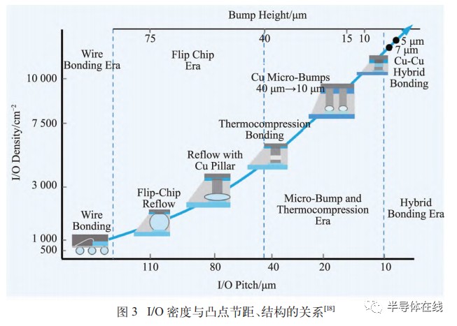
The relationship between I/O density, convex pitch, and structure is shown in Figure 3. Traditional controllable collapse chip connection solder balls can no longer meet the requirements of high-end performance packaging for high-density I/O, and instead, pitch is less than 100 μ The micro convex point of m. At present, the commonly used micro convex point connection structures include copper tin copper, nickel tin nickel, copper tin nickel, copper nickel tin nickel copper, and copper copper. In the hot pressing bonding process, the minimum pitch of micro protrusions can even be reduced to 10 μ m. The hybrid bonding process results in a convex pitch less than 10 μ M. In addition to hybrid bonding between wafers, C2C and C2W hybrid bonding technology has been favored in recent years. In addition to achieving optimal electrical performance, this technology can choose known qualified chips for SMT to improve overall yield and reduce manufacturing costs. Due to the involvement of wafer cutting in the hybrid technology of C2C and C2W, the issue of how to protect the surface of the chip after chemical mechanical polishing from contamination and improve the strength of the bonding interface still needs to be solved. Existing reports have shown that during the cutting process, photoresist is used to cover the surface of the chip, followed by plasma post-treatment. However, the packaging yield of the product still cannot meet the requirements of industrial mass production, and further research is needed to address these issues.
4.2 High density wiring for high-end performance packaging
In terms of high-density wiring, 2.5D and 3D packaging can share mature processes with front-end wafer manufacturing, with line width/spacing below the micrometer level, achieving the highest wiring density. The 2D, 2.1D, 2.2D, and 2.3D packaging based on FO is closer to the process of packaging and testing enterprises. FO embeds chips into molded materials to reconstruct wafers. A large amount of molded materials not only hinders device heat dissipation, but also causes thermal mismatch with the chips, resulting in severe wafer warping. At the same time, the polymer dielectric layer wrapped in metal wiring exacerbates this phenomenon, posing significant challenges to the process. In addition to wafer warping, the molded plastic shrinks during the forming process, causing the chip to deviate from the set position, resulting in exposure deviation, which is not conducive to the production of high-density wiring and requires new equipment investment. As an important connection structure for FO packaging, high-density wiring also faces high technical difficulties. Especially in the production process of multi-layer wiring, the arching of the bottom layer wiring hinders the exposure and etching of the upper layer photoresist, causing wiring defects. Metal wiring can also cause detachment from the dielectric layer due to excessive etching of the seed layer after electroplating. Currently, in the FO packaging structure, the 4-layer wiring width/spacing is 5 μ M/5 μ The product of m has entered the mass production stage, and the size limit of wiring width/spacing is 1 μ M/1 μ m. The maximum number of layers is 6, which makes it difficult to meet the connection between chips with higher I/O density. According to reports, some scholars have used the Damascus process of polyimide to produce submicron wiring and increase the number of dielectric layers, but the above research has not been widely applied in mass production.
4.3 Intermediate layer for high-end performance packaging
In high-end performance packaging, the intermediate layer, as an important connection structure, can significantly improve the integration of chips. At present, the intermediate layer is divided into organic intermediate layer and inorganic intermediate layer according to material composition. Among them, the organic intermediate layer mainly uses polymer materials to make high-density wiring, which is placed between the chip and the substrate as a cheap alternative to 2.5D silicon adapter boards. At the same time, it reduces the difficulty of manufacturing thin wire wide/narrow spacing wiring on the substrate, such as Samsung's board level packaging adapter board and TSMC's FO based integrated substrate.
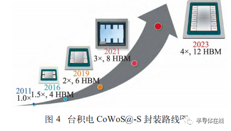
The inorganic intermediate layer includes a silicon bridge, a silicon adapter plate, and a glass adapter plate. There are local high-density connections between high bandwidth storage chips and processing chips. Intel has developed a silicon bridge structure based on the above structural characteristics, which is embedded in the substrate and only connects the high-density I/O part. The remaining wiring connections are completed by the substrate. Some companies combine silicon bridges with FO packaging to develop new packaging structures. According to reports from Sun and Moon, the wiring width/spacing is 0.8 μ M/0.8 μ Compared to the 2.5D packaging of m, using a wiring width/spacing of 2 μ M/2 μ The fanout type chip packaging (FOCoS-B) with embedded silicon bridges on m exhibits better electrical performance. In 2.5D packaging, the silicon adapter board provides a medium for chip plane interconnection. TSMC CoWoS@-S The packaging route is shown in Figure 4. According to the combination method of TSMC's storage chip and logic chip, the planar area of the silicon adapter board will reach four times that of the 2011 adapter board in 2023. However, the problem of how to attach large-sized adapter boards to the substrate without chip offset and virtual soldering remains to be solved. In addition, silicon, as a semiconductor material, is not conducive to signal transmission and integrity maintenance. TSMC compensates for the above shortcomings by producing capacitors on silicon adapter boards, but the capacitance formed by metal wiring is limited and cannot meet the wide application needs. In recent years, some scholars have proposed using insulation materials such as glass to replace silicon, and further exploration is needed to make multi-layer submicron level wiring on glass adapter plates and improve integration.
In high-end performance packaging, products often adopt a stacked structure and there are a large number of microstructures used for signal connection, which makes the packaging body have characteristics such as multiple materials, multiple interfaces, and large size span, posing significant challenges in thermal, mechanical, and electrical aspects.
5.1 Thermal mismatch issues in high-end performance packaging
In high-end performance packaging, thermal mismatch between silicon, metal, and polymer materials is a common problem, which leads to solder ball fatigue, mold plastic cracking, and bottom filler interface delamination at the corners of the packaging structure. The failure phenomenon of 2.5D packaging structure is shown in Figure 5. Among the above issues, FO packaging has advantages in reducing the thermal fatigue of solder balls. A large amount of molded plastics increases the thermal expansion coefficient of the structure to the level of the substrate, and the two maintain coordinated deformation during thermal expansion and contraction. The stress of solder balls is reduced, making the structure perform well in reliability testing. At the same time, the small proportion of molded plastics reduces the inertia of solder balls during vibration and drop, which helps to maintain the integrity of the packaging structure during the above tests. Compared to FO packaging, the stacked structures of 2.5D and 3D packaging are inherently significant, which not only hinders heat dissipation but also increases the difficulty of coordinating deformation with the substrate. The increasing size of 2.5D silicon adapter plates exacerbates this phenomenon. In addition, using molded plastics for external protection of FO, 2.5D, and 3D packaging products may cause cracking of the molded plastic due to thermal mismatch between the silicon chip and the molded plastic. Using finite element tools to select the material of the molded plastic in advance is a suitable solution.

5.2 Thermoelectric migration of microstructures
With the continuous reduction of packaging size, micro bumps and high-density wiring, as important electrical connection structures for high-end performance packaging, have increasingly prominent thermoelectric migration issues. In 2.5D and 3D packaging of high-performance products, the diameter of micro bumps (10-20) μ m) Shrink by one order of magnitude compared to traditional solder balls. Under low current conditions of 0.05 A, the current density through the cross-section of the structure is approximately 104A/cm2, approaching the threshold for tin layer electromigration. In addition, during the service process of the product, tin and silver in the structure will be completely converted into intermetallic compounds, causing volume shrinkage and Kirkendall pores, accelerating the failure of the structure. The SEM image of the micro convex point cross-section in the electromigration test is shown in Figure 6.
Similar to the thermoelectric migration of micro convex points, the high-density wiring between the processing chip and the high bandwidth storage chip also suffers from the above-mentioned problems, and the temperature gradient between the processing chip and the storage chip accelerates the occurrence of the above phenomenon when the processing chip operates at a temperature of up to 100 ℃. In FO packaging, the metal copper wiring is wrapped in a polymer passivation layer, causing surface oxidation and the generation of copper oxide. The oxidation failure of copper wiring is shown in Figure 7. During the process of copper oxidation, copper continuously migrates to the surface, resulting in a large number of pores at the interface between copper and copper oxide. Under the action of high temperature and high current, the above oxidation phenomenon becomes more obvious, forming a large number of pores that seriously affect the wiring strength and signal transmission. Some studies use non organic materials to form a protective layer on the surface of copper, isolating it from polymer materials to prevent oxidation, resulting in new processes that increase additional manufacturing costs.

5.3 Heat dissipation issues of packaging bodies
In pursuit of optimal computing performance, the technology nodes of processing chips are constantly advancing, and the number of integrated transistors is increasing rapidly. At the same time, the integration degree of packaging is further improved, requiring the packaging body to provide heat dissipation energy with a heat flux density of up to 1000 W/cm2 for processing chips. In high-end performance packaging, UHD FO, 2.5D, and 3D packaging ultimately adhere to the substrate, and the general assembly method is Flip Chip Ball Grid Array (FCBGA). The main heat dissipation pathway for this package is the back heat sink. Some scholars have optimized its design by using water cooling, gas-liquid two-phase, air cooling, and other methods to dissipate heat. The relationship between the maximum heat dissipation power (Qmax) and the effective heat transfer coefficient (heff) of the structure has been optimized to meet the application needs of different products. The main pathway for heat dissipation is shown in Figure 8.

Another important factor affecting heat dissipation in FCBGA structures is the selection of thermal interface materials. Compared to traditional siliceous materials, low melting point metal materials such as indium, indium silver, tin, and liquid metals are more favored. These materials have a higher thermal conductivity and can timely transfer heat during chip processing. However, reflow soldering of substrate solder balls will cause these low melting point materials to melt again, resulting in hole and overflow problems that need to be effectively solved. To further meet the demand for heat dissipation, more high-quality thermal interface materials, such as graphite, need to be developed. In addition to the selection of heat sink and thermal interface materials mentioned above, some researchers have also achieved partial thermal performance improvements by optimizing the stacking method of logic chips and storage chips, as well as the cavity size of FCBGA.
The rapid development of fields such as high-performance computing, artificial intelligence, cloud computing, data centers, and 5G communication has driven chip technology towards high performance and high bandwidth, resulting in the continuous advancement of single SoC technology nodes, increasingly complex integration functions, and rising manufacturing costs. Some manufacturers separate the storage and processing units of SoC, and then recombine them through UHD FO, 2.5D, and 3D packaging methods to achieve optimal computing performance. High end performance packaging can better meet the growing requirements of I/O density and heat dissipation capacity of processing chips, and is expected to receive more attention and research.
Information source: Semiconductor Online
(The above article is a reprint. If there are any copyright or other issues, please contact us for assistance.)


 Tel:18018712764
 E-mail:huangtz@tec-pho.com
 Address:3rd Floor, Building B, No. 84 Xinyu Road, Xinqiao Street, Bao'an District, Shenzhen City, Guangdong Province
About Us
· Company culture
· Honor
Product
· Probe station
· Chip testing machine
· Blue film braiding machine
· LED spectrophotometer
· More products
News
· Company News
· Industry News
Contact
· Online Message

Website registration:粤ICP备12034829号
Copyright© 2024 Tec Semiconductor Equipment (Shenzhen) Co., Ltd

点击右上角
分享给朋友吧


