


Advanced packaging substrate technology
Time: 2023-04-15 09:20:12
Click:
IC packaging substrate is an important component of semiconductor packaging material, used to carry the chip, provide electrical connection, protection, support and heat dissipation for the chip. In order to achieve the system-level integration requirements of 3D-SiP, to meet the needs of high-end applications such as 5G and high-performance computers in the future
IC packaging substrate is an important component of semiconductor packaging material, used to carry the chip, provide electrical connection, protection, support and heat dissipation for the chip. In order to realize the system-level integration requirements of 3D-SiP and meet the needs of high-end applications such as 5G and high-performance computers in the future, the industry has put forward the requirements of improving the wiring density, reducing the line width and line distance, reducing the size and weight, and improving the thermal performance of the advanced substrate. At present, the research directions of advanced packaging substrate mainly include process improvement, fine wiring, flip chip ball grid array packaging substrate (FCBGA), core-less packaging substrate, and embedded substrate of active and passive devices.
1.FCBGA(Flip Chip Ball Grid Array)
FCBGA is the most important package format for graphics acceleration chips. This packaging technology began in the 1960s, when IBM developed the so-called C4(Controlled Collapse Chip Connection) technology for the assembly of large computers, Subsequently, it was further developed that the surface tension of the fused convex block could be used to support the weight of the chip and control the height of the convex block, and became the development direction of flip technology.
The advantages of FCBGA are as follows: The first point is to solve electromagnetic compatibility (EMC) and electromagnetic interference (EMI) problems. In chips with Wire Bond packaging technology, the signal transmission is carried out through a metal wire with a certain length, which produces an impedance effect at high frequencies. However, FCBGA uses small balls instead of the original pins to connect the processor, using this package not only provides excellent electrical performance, but also reduces the loss and inductance between component interconnects, reduces the problem of electromagnetic interference, and can withstand higher frequencies. The second is to increase the density of I/O. Generally speaking, the I/O leads using WireBond technology are arranged around the chip, but after the FCBGA package, the I/O leads can be arranged in an array on the surface of the chip, providing a higher density I/O layout, resulting in the best use efficiency. Inversion technology reduces the area by 30% to 60% compared to traditional packaging forms. The third point is based on the unique flip package form of FCBGA, the back of the chip can be exposed to air, can directly heat. At the same time, the substrate can also improve the heat dissipation efficiency through the metal layer, or install a metal heat sink on the back of the chip, further strengthen the heat dissipation ability of the chip, and greatly improve the stability of the chip at high-speed operation.

Image credit :CSDN
2. Coreless packaging substrate
According to whether there is a core board, the IC package substrate can be divided into a core substrate and a core free substrate. It uses Polyimide (PI) with double-sided copper foil as the substrate,PI film as the insulation layer, through addition method to achieve high density wiring. The thickness of the coreless package substrate is only 1/3 of the thickness of the traditional substrate, and the thickness is reduced, which not only makes the coreless substrate more suitable for the trend of light, thin, short and small consumer electronics products, but also makes it have higher signal transmission speed, better signal integrity, lower impedance, more free wiring design, and can achieve finer graphics and spacing. However, due to the lack of mechanical support of the steel core plate, the coreless packaging substrate is weak and easy to warp. How to reduce warping during manufacturing and assembly has become an important topic in the field of research and production of coreless packaging substrates. Common ways to reduce the warpage of coreless packaging substrates are: Adding glass fiber to the semi-cured sheet to increase the stiffness, replacing the dielectric material on the surface of the substrate with a stiffer semi-cured sheet, using a dielectric material with low thermal expansion coefficient to reduce warping caused by the mismatch of thermal expansion coefficient between the Cu line and dielectric material, developing suitable fixtures for the process to reduce warping, Balance the copper coating rate of each layer of substrate to reduce the mismatch of thermal expansion coefficient of upper and lower layers. The following figure shows a coreless packaging substrate fabrication method.
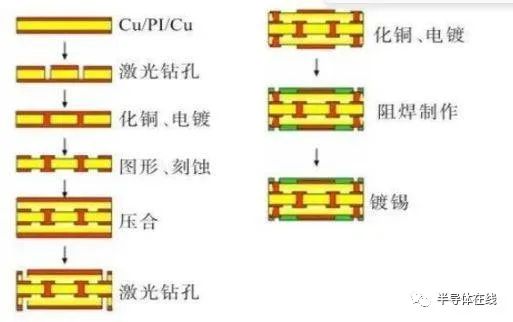
Photo source: Zhihu
3. Embedded substrate
According to the types of Embedded components, it can be roughly divided into passive component embedding, active device embedding, passive and active mixed embedding technology and Intel's Embedded Multi-die Interconnect Bridge (EMIB) technology.
3.1 Passive components embedded in substrate technology
Compared with the traditional technology of welding all components to the surface of the PCB board, the component embedding technology has four advantages. The first point is that the flexibility and freedom of PCB design and wiring can be increased, and the length of wiring can be reduced and shortened, thus greatly improving the degree of PCB high-density. The second point is to improve the high reliability of PCB assembly, through this process method, it is extremely obvious to reduce the welding points of the PCB surface, thus improving the reliability of the assembly board, greatly reducing the probability of failure caused by welding points. The third point is to improve the electrical performance of the PCB assembly, which is because the passive component is buried in the high-density PCB, eliminating the connection pad, wire and its own lead required for the discrete passive component to form a loop after welding. The fourth point is very obvious savings in product or PCB assembly costs.
3.2 Technology of embedding active devices into substrate
According to the sequence of chip embedding process, active device embedding technology can be divided into chip first (chip-first) embedding technology and chip last embedding technology. Chip-first embedding technology first buries the chip in an organic insulating medium, and then makes a circuit pattern to realize signal transmission and power supply. In the post-chip embedding technology, a build-up substrate is first made, a slot is cut on the prepared substrate and a circuit pattern is made, the chip is placed in the slot to achieve electrical connection, and then the gap between the chip and the slot is filled with resin.
Compared with the chip-first technology, the chip embedded in the ChIP-last technology is located on the top layer of the substrate, can be reworked and better heat dissipation, and there is no other substrate layer process step after embedding the chip, and the processing yield is higher. However, the chip-first technology also has its advantages. The post-chip technology can only bury one layer of chips in the chip, and the substrate surface of the embedded chip can not be mounted again, so the longitudinal utilization rate of the substrate space is better than that of the post-chip technology.
3.3EMIB Technology
EMIB is an ultra-thin silicon wafer with a multi-layer conductive metal (Back End Of Line, BEOL) interconnect embedded in the top layer of the organic package substrate, through the connection of the solder ball and the reverse chip, to achieve local high density interconnect between two or more chips. This embedded structure can be placed anywhere on the organic substrate to achieve ultra-high density local interconnections, integrating large chips in a much larger size range than typical mask plates, allowing for very flexible use. The following diagram shows the EMIB technology structure.

Image credit: Semiconductor Technology
(The above article is reprinted, if there are copyright and other issues, please contact us to deal with)


 Tel:18018712764
 E-mail:huangtz@tec-pho.com
 Address:3rd Floor, Building B, No. 84 Xinyu Road, Xinqiao Street, Bao'an District, Shenzhen City, Guangdong Province
About Us
· Company culture
· Honor
Product
· Probe station
· Chip testing machine
· Blue film braiding machine
· LED spectrophotometer
· More products
News
· Company News
· Industry News
Contact
· Online Message

Website registration:粤ICP备12034829号
Copyright© 2024 Tec Semiconductor Equipment (Shenzhen) Co., Ltd

点击右上角
分享给朋友吧


